

Sony’s Semiconductor division has announced that it successfully developed the world’s first stacked CMOS image sensor technology with two-layer transistor pixels that grants double the light gathering capability.
Sony explains that typical image sensors place photodiodes and pixel transistors on the same substrate, but in this new design, it was able to separate them onto different substrate layers. The result is a sensor that approximately doubles the saturation signal level — basically its light gathering capability — which dramatically improves the dynamic range and reduces the noise
Saturation signal level isn’t directly a sensor’s light-gathering capability but is a major gating factor that influences how accurately a sensor is able to interpret light information in dim environments. For the sake of basic explanation, double the light gathering ability is the end result of this advancement.
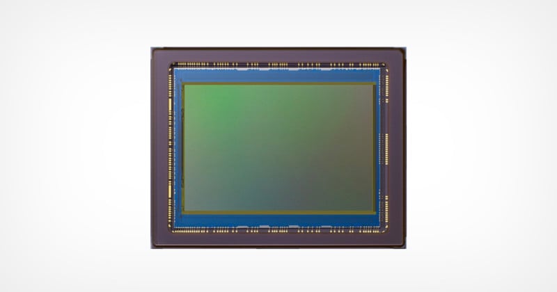
Typical stacked CMOS sensors use a structure of a pixel chip made up of back-illuminated pixels stacked on top of a logic chip where signal processing circuits are formed. Within each chip, photodiodes that convert the light to electrical signals and pixel transistors that control the signals are situated next to each other on the same layer.
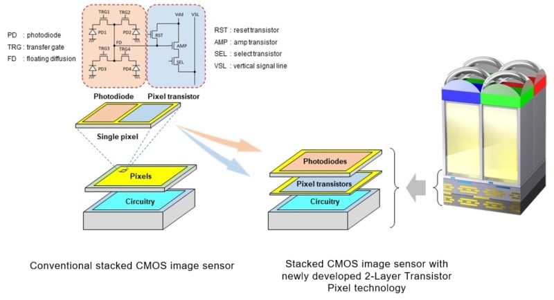
Sony’s new architecture is an advancement in stacked CMOS image sensor technology that separates the photodiodes and pixel transistors onto separate substrates that are stacked on top of each other, rather than side-by-side. Sony says that the new stacking technology enables the adoption of architectures that allow the photodiode and pixel transistor layers to each be optimized, thereby approximately doubling saturation signal level relative to conventional image sensors and, in turn, widening dynamic range.
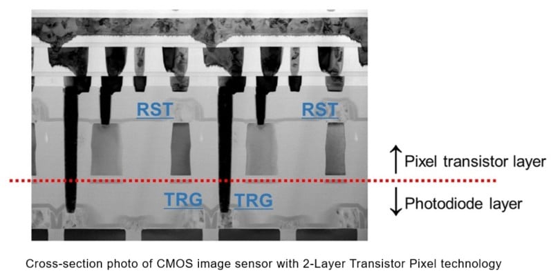
“Additionally, because pixel transistors other than transfer gates (TRG), including reset transistors (RST), select transistors (SEL) and amp transistors (AMP), occupy a photodiode-free layer, the amp transistors can be increased in size,” Sony says. “By increasing amp transistor size, Sony succeeded in substantially reducing the noise to which nighttime and other dark-location images are prone.”
The result for photography means wider dynamic range (better exposure in photos with harsh backlighting or in dim settings) and lower noise in photos that are taken in dark environments. Sony specifically notes that this technology is going to make for increasingly high-quality imaging in the case of smartphone photography. The new technology’s pixel structure will enable pixels to maintain or improve their existing properties at not only current but also smaller pixel sizes.
That last note is particularly important, as it signals that Sony believes it has found a way to markedly improve the photo quality of smartphone sensors. In short, the quality of mobile photography could very well see a huge leap in performance thanks to this breakthrough.
Sony doesn’t specify when it plans to manufacture sensors at scale using this technology but does say it will continue to iterate on the design to further increase image quality in sensors large and small.
Author: Jaron Schneider
Source: Petapixel
